- 您现在的位置:买卖IC网 > Sheet目录1994 > DS1677E (Maxim Integrated Products)IC CTRLR SYSTEM PORT 20-TSSOP
DS1677
10 of 18
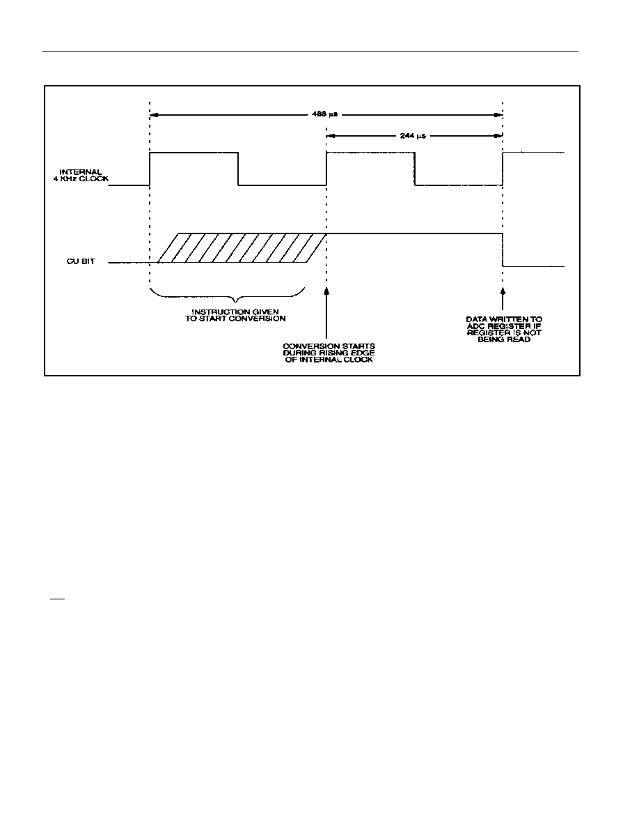
CU BIT TIMING Figure 5
3-WIRE SERIAL INTERFACE
Communication with the DS1677 is accomplished through a simple 3-wire interface consisting of the
Chip Select (CS), Serial Clock (SCLK) and Input/Output (I/O) pins.
All data transfers are initiated by driving the CS input high. The CS input serves two functions. First, CS
turns on the control logic, which allows access to the shift register for the address/command sequence.
Second, the CS signal provides a method of terminating either single byte or multiple byte (burst) data
transfer. A clock cycle is a sequence of a rising edge followed by a falling edge. For data input, data must
be valid during the rising edge of the clock and data bits are output on the falling edge of the clock. If the
CS input goes low, all data transfer terminates and the I/O pin goes to a high impedance state.
Address and data bytes are always shifted LSB first into the I/O pin. Any transaction requires the
address/command byte to specify a read or write to a specific register followed by one or more bytes of
data. The address byte is always the first byte entered after CS is driven high. The most significant bit
( RD /WR) of this byte determines if a read or write will take place. If this bit is 0, one or more read cycles
will occur. If this bit is 1, one or more write cycles will occur.
Data transfers can occur one byte at a time or in multiple byte burst mode. After CS is driven high an
address is written to the DS1677. After the address, one or more data bytes can be read or written. For a
single byte transfer one byte is read or written and then CS is driven low. For a multiple byte transfer,
multiple bytes can be read or written to the DS1677 after the address has been written. Each read or write
cycle causes the register address to automatically increment. Incrementing continues until the device is
disabled. After accessing register 0Eh, the address wraps to 00h.
Data transfer for single byte transfer and multiple byte burst transfer is illustrated in Figures 6 and 7.
发布紧急采购,3分钟左右您将得到回复。
相关PDF资料
DS1678S/T&R
IC RECORDER REALTIME EVENT 8SOIC
DS1682S
IC TIMEKEEPER ALARM ELAPSE 8SOIC
DS1683S+T&R
IC REAL TIME EVENT REC 8SOIC
DS1685EN-5/T&R
IC RTC 5V 64BIT Y2K IND 24TSSOP
DS1688S+
IC RTC W/NV RAM CTRL 28-SOIC
DS1689SN+T&R
IC RTC SER NV RAM CTRL IN 28SOIC
DS17285S-3NT
IC RTC 3V 2K NV RAM 24-SOIC
DS1742-100IND
IC RTC RAM Y2K 5V 100NS 24-EDIP
相关代理商/技术参数
DS1677E+
功能描述:实时时钟 Portable System Controller RoHS:否 制造商:Microchip Technology 功能:Clock, Calendar. Alarm RTC 总线接口:I2C 日期格式:DW:DM:M:Y 时间格式:HH:MM:SS RTC 存储容量:64 B 电源电压-最大:5.5 V 电源电压-最小:1.8 V 最大工作温度:+ 85 C 最小工作温度: 安装风格:Through Hole 封装 / 箱体:PDIP-8 封装:Tube
DS1677E-5
制造商:未知厂家 制造商全称:未知厂家 功能描述:Portable System Controller(275.85 k)
DS1678
功能描述:实时时钟 Real-Time Event Recorder RoHS:否 制造商:Microchip Technology 功能:Clock, Calendar. Alarm RTC 总线接口:I2C 日期格式:DW:DM:M:Y 时间格式:HH:MM:SS RTC 存储容量:64 B 电源电压-最大:5.5 V 电源电压-最小:1.8 V 最大工作温度:+ 85 C 最小工作温度: 安装风格:Through Hole 封装 / 箱体:PDIP-8 封装:Tube
DS1678+
功能描述:实时时钟 Real-Time Event Recorder RoHS:否 制造商:Microchip Technology 功能:Clock, Calendar. Alarm RTC 总线接口:I2C 日期格式:DW:DM:M:Y 时间格式:HH:MM:SS RTC 存储容量:64 B 电源电压-最大:5.5 V 电源电压-最小:1.8 V 最大工作温度:+ 85 C 最小工作温度: 安装风格:Through Hole 封装 / 箱体:PDIP-8 封装:Tube
DS1678J
制造商:未知厂家 制造商全称:未知厂家 功能描述:2-Input Digital Multiplexer
DS1678J/A+
制造商:未知厂家 制造商全称:未知厂家 功能描述:2-Input Digital Multiplexer
DS1678K
功能描述:KIT EVAL RT EVENT RECORD DS1678 RoHS:否 类别:编程器,开发系统 >> 过时/停产零件编号 系列:- 标准包装:1 系列:- 传感器类型:CMOS 成像,彩色(RGB) 传感范围:WVGA 接口:I²C 灵敏度:60 fps 电源电压:5.7 V ~ 6.3 V 嵌入式:否 已供物品:成像器板 已用 IC / 零件:KAC-00401 相关产品:4H2099-ND - SENSOR IMAGE WVGA COLOR 48-PQFP4H2094-ND - SENSOR IMAGE WVGA MONO 48-PQFP
DS1678S
功能描述:实时时钟 RoHS:否 制造商:Microchip Technology 功能:Clock, Calendar. Alarm RTC 总线接口:I2C 日期格式:DW:DM:M:Y 时间格式:HH:MM:SS RTC 存储容量:64 B 电源电压-最大:5.5 V 电源电压-最小:1.8 V 最大工作温度:+ 85 C 最小工作温度: 安装风格:Through Hole 封装 / 箱体:PDIP-8 封装:Tube